^Junction diode
^Junction diode
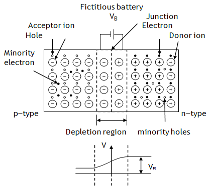
It is formed by joining p-type crystal with a n-type crystal. Majority charge concentration gradient across junction diffuses majority charge carriers diffusion from p to n (called diffusion current) & combine with each other near the junction and get neutralised. Due to electron hole neutralization near the junction the impurity atoms become uncovered & a thin region of uncovered unbalanced immobile charges is created. This region is called depletion region (thickness » 1 μm). This resulting in potential gradient across junction which drifts minority charge carriers drifting from n to p (called drift current). Initially, diffusion current is large and drift current is small. As the diffusion process continues, the space-charge regions on either side of the junction extend, thus increasing the electric field strength. This electric field (» 106 V/m) offers a barrier (called potential barrier, it depends upon the nature of the SC (e.g. 0.7 V for Si & 0.3 V for Ge), the temperature of SC & the amount of doping) to the further diffusion of e–s & holes towards each other but increases the drift current till the steady state (i.e. until the diffusion current equals the drift current & thus no net current flows or the diode doesn’t conduct).